Zachary Lamport, PhD Candidate
Public Presentation in ZSR Library, Room 404
Thursday, April 19, 2018, at 10:30 AM
Oana Jurchescu, PhD, Advisor
The defense will follow.
ABSTRACT
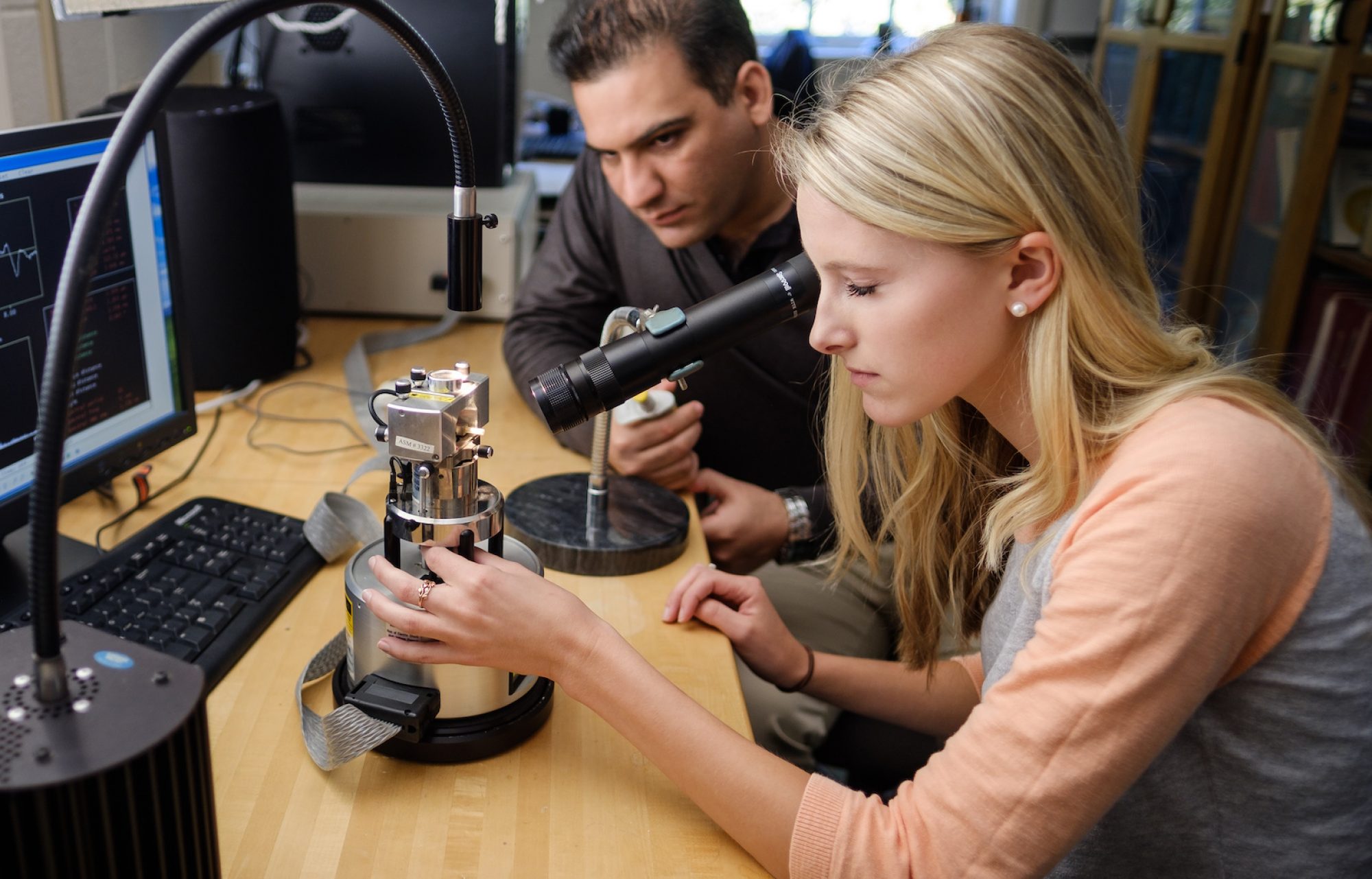
The electrical properties of devices based on an organic compound result from the structure of the molecules, their solid-state packing, efficiency of charge injection from the electrodes, and the fabrication procedures. The length scales of interest can also vary widely, ranging from a few nanometers in the case of charge transport through single molecules or two-dimensional molecular ensembles, to tens of micrometers in devices focusing on thin films or molecular crystals. The work outlined in this thesis examines the characteristics of electronic devices at both extremes by incorporating organic molecules in molecular rectifiers and organic field-effect transistors (OFETs).
We successfully designed and fabricated molecular rectifiers based on self-assembled monolayers and identified relevant structure-function relationships. We elucidate the dependence of the rectification behavior on molecular length and structure, and found that the degree of rectification is enhanced in shorter molecules and linearly dependent on the strength of the molecular dipole moment. We further developed compounds that, when included into the molecular diodes, rectified current by as much as three orders of magnitude depending on their structure. This performance is on par with that of the best molecular rectifiers obtained on a metallic electrode, but it has the advantage of lower cost and more efficient integration with current silicon technologies, which may yield hybrid systems that can expand the use of silicon towards novel functionalities governed by the molecular species grafted onto its surface.
We then explored charge transport in OFETs using the organic semiconductor 7,14-bis(trimethylsilylethynyl)benzo[k]tetraphene (TMS-BT). We produced thin-film OFETs which exhibited more efficient electronic transport than single crystal devices of the same material, in spite of the inherent presence of grain boundaries. We explained these findings in terms of charge transport anisotropy and electronic trap formation at the interface between the semiconductor and dielectric. We further reduced aggressively the contact resistance in small molecule and polymer OFETs by varying the metal deposition rate, which resulted in over 5 times improved charge carrier mobility compared with the best reported devices with identical composition and structure. The obtained contact resistance normalized over the channel width was 500 Ωcm, and the corresponding devices exhibited charge carrier mobilities of 19.2 cm2/Vs for 2,8-difluoro-5,11-bis(triethylsilylethynyl) anthradithiophene (diF-TES ADT) and 10 cm2/Vs for indacenodithiophene-co-benzothiadiazole copolymer (C16IDTBT), with minimal dependence on the gate voltage.